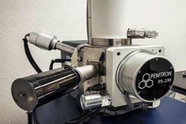
Nanounity Introduces The Pemtron Range Of Compact Scanning Electron Microscopes

Nanounity announces their appointment to distribute the Pemtron range of scanning electron microscopes. The compact Pemtron system has been designed to bridge the gap between tabletop and full size tungsten SEMs.
Santa Clara, CA (PRWEB) - Tabletop SEMs are inexpensive and easy to use compared to standard size SEMs but have limited performance and capability such as small sample sizes, lower magnifications and lower resolution. Full size SEMs would normally provide better imaging performance and more analytical capability but generally require more knowledge to operate and have a higher cost of maintenance. The Pemtron PS-230 and PS-250 SEMs address the gap between these two types of SEM product, offering competitive prices compared with higher end tabletop SEMs, are easy to use and have a low cost of maintenance while equalling or exceeding the performance of a full size SEM.
In choosing to offer Pemtron’s products, Nanounity studied the market-place for SEMs. Describing what was found, Nanounity director, Brad Rangell, said “We ran across many people who were evaluating or have recently purchased tabletop SEMs. Our observations suggest that many users have applications that require performance beyond a tabletop system. In many cases, the determining factor to buy a tabletop SEM is price. The user might have higher performance needs but, with a limited budget, is forced into selecting a system with added capabilities and options.”
Continuing, Rangell noted “At the other end of the scale, the full size tungsten SEMs may accept a variety of sample sizes and offer higher magnification and resolution. These systems usually offer a number of options such as motorized stages, low vacuum, sample airlocks and ports for external analytical devices. These options raise the purchase price and make the system out of reach to buyers with limited budgets. Full size SEMs are generally larger, take up more floor space, have special facilities requires and use water chillers to cool the lens. This ultimately raises the price and cost of ownership.”
The Pemtron systems provide a compact solution for SEM users combining the attributes of a full size SEM at approximately the price of a high end tabletop system. A PS-230 system has a 5-axis motorized stage, accepts larger samples and has higher magnification (up to 300,000x) and superior resolution (3 nm at 30 kV). The cost of ownership is also reduced as Pemtron systems do not need a water chiller or have special facility requirements. Adding analytical capability is readily available as Pemtron offers compatibility with many industry-leading energy dispersive spectrometers (EDS) including those from Bruker, Oxford Instruments and EDAX. A back scattered electron detector (BSED) is also offered. With extra ports, Pemtron systems are designed to accommodate in-situ techniques such as nanoindenters and nanomanipulators making the Nanounity offering versatile and cost–effective for the discerning electron microscopist. For details on Pemtron’s family of compact SEM systems, please visit http://www.nanounity.com/ and learn about all of Nanounity’s products & solutions.
About Nanounity
Nanounity supplies surface science analytical solutions through a range of synergistic products through partnerships with leading instrumentation manufacturers. The core technologies are microscopy, metrology and spectroscopy. Through the strong personal commitment of the founders, Nanounity has built a strong reputation in the USA and Asia providing high standards of materials knowledge enabling the Company to match the requirements of users to a range of tools and techniques. Backed with applications knowledge and customer service support, Nanounity offers experience and skills to help deliver innovative products of the highest performance at affordable prices.
Nanounity’s product profile delivers solutions to researchers, engineers and scientists in many disciplines: from data storage, semiconductors, polymers, material science and the life sciences. These tools include compact SEMs, correlative microscopy combining fluorescence imaging with SEM, optical profilers and nanomechanical testing systems that incorporate nano-hardness testing with surface topography. For details on Nanounity and all its products & solutions, visit http://www.nanounity.com.
Source: PRWeb
View original release here: http://www.prweb.com/releases/2013/6/prweb10847941.htm
