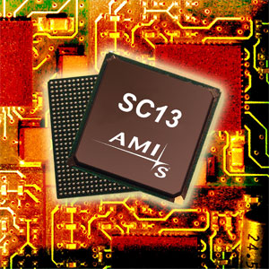
AMI Semiconductor To Lead The Industry In FPGA-to-ASIC Conversions
 Pocatello, ID - AMI Semiconductor, Inc. (AMIS) recently announced the capability to convert 1.2 volt, 90nm FPGAs to 130nm cell-based ASICs. This competency supports OEMs moving from expensive, high-density FPGAs for prototyping to more cost-effective ASICs for production.
AMIS is believed to be the first company to provide drop-in replacement components for Altera and Xilinx 90nm FPGAs targeting communications (wired and wireless telecom and datacom) and military/commercial avionics application-markets. AMIS ASICs match the core voltage, package and IP of the original FPGAs, reducing customer costs and power consumption as they move from prototype to production silicon.
"Many design engineers select FPGAs for prototyping, but once their product is ready to move into production they find that conversion to cost-effective ASICs can be painful, time consuming and expensive. We are the partner that takes the pain out of FPGA-to-ASIC drop-in conversions with our flexible design interface and key IP functions," said Mike O'Neill, senior vice president of structured digital products at AMI Semiconductor. "Our customers are increasingly taking advantage of our hybrid design flow to combine FPGA sub-system prototypes with ASIC IP to create highly integrated ASIC solutions." Their standard cell product technology supports a wide range of I/O standards including SSTL, HSTL, LVPECL, and LVDS. Memory compilers and register file memories with integrated BIST and redundancy support a wide range of sizes and applications. High-speed, low-jitter PLLs are integrated with clock-tree synthesis to support high-performance system operation. Advanced digital clock management functions employing DLL technology will complete the FPGA timing generator conversion capability. DDR2 PHYs and controllers interface to industry-standard off-chip memories. PCI-Express SerDes running at 2.5Gbps will be supported from the physical layer to the transaction layer via the PIPE interface. A full range of 32-bit processors and supporting peripherals are available to round out the product offering. Moving forward, the IP portfolio will grow to include Gigabit Ethernet, XAUI, USB 2.0, and other high-speed interfaces.
In addition to supporting a traditional RTL design flow, inputs from a variety of sources can be accepted as well, including RTL designs and netlists targeting other ASIC and FPGA technologies. AMI Semiconductor's hybrid design flow includes full design for test (DFT) capability for at-speed test, memory BIST, timing-driven layout, clock-tree synthesis, and signal-integrity checking.
SOURCE: AMI Semiconductor, Inc.
